Metrology in additive manufacturing: Inspection and design compensation
Written by nTop
Published on December 14, 2022
Additive manufacturing is creating new possibilities for designing advanced products, but there are still challenges to overcome to ensure quality of advanced applications—from aerospace to medical. In this article, we explore how to take advantage of the latest metrology technologies.
As design for additive manufacturing (DfAM) increases in popularity, we are able to create more innovative and effective designs. The medical device industry can use additive manufacturing (AM) and its design freedom benefits to develop patient-specific devices to improve patient outcomes.
However, when designing for additive manufacturing, engineers face the challenge of designing and measuring lattice structures that promote bone growth in implants. This article will explore this challenge, covering how to perform metrology measurements with X-Ray Computed Tomography (XCT), and compensating for surface roughness and defects.
Metrology measurements challenges in AM
With the rise of design for additive manufacturing awareness, more efficient and functional designs are being made, taking advantage of additive manufacturing complexity. However, at the same time, since these designs are usually complex enough not to be manufactured using conventional manufacturing methods, they are also complex enough not to be measurable using conventional metrology tools.
To tackle this challenge, you can use a non-conventional metrology tool called X-Ray Computed Tomography. While XCT still lacks standardization and needs more research to better generate uncertainty statements, it is becoming increasingly popular in the AM field.
Much of the work in AM for medical devices involves biomimetic design. We have known for a long time now that nature is the best designer, and attempting to mimic nature's creations can often help us achieve our design objectives.
However, manufacturing these nature-inspired designs creates a challenge — how do we measure these designs, which may have complex internal and external features? An intricate lattice structure, for example, can be complicated to measure with conventional processes. Metrology provides a solution to this challenge, but it requires that you design with metrology in mind.
Metrology and XCT basics
What is metrology?
Metrology is “the science of measurement” and has three overlapping activities:
- Scientific metrology is the fundamental establishment of units of measurement.
- Industrial metrology ensures the adequate application of developed measurements and instruments in the industry.
- Legal metrology provides the harmonizations and legal statuary requirements for measurements.
What is design for metrology?
When you design for metrology, you must consider how you will attempt to measure the essential features of your design.
Depending on the nature of the feature, you might opt for a contact measurement, which requires that the feature is accessible, or an optical measurement, which requires a direct line of sight to that feature. If the feature isn't accessible or is too complex, you may need to leverage XCT.
What is XCT?
X-Ray Computed Tomography is a nondestructive technique that allows you to visualize the interior features of solid objects and obtain information on their 3D properties and geometries.
In XCT, multiple x-ray transmission images are taken by rotating the examined object 180° or 360° within the instrument. Using a specialized algorithm, the side-view, two-dimensional projection images come together to create a set of horizontal cross-sectional images. When combined, this results in a three-dimensional representation of the object.
XCT is a flexible, innovative, non-contact measurement technology that can reveal the internal details of parts in three dimensions, which is why it has become a vital tool in coordinate metrology.
Should you use XCT?
XCT is an essential DfAM tool. AM designs often have complex shapes and non-accessible internal features. In many cases, it isn’t possible to inspect AM parts with traditional measurement technologies without cross-sectioning them. XCT resolves this issue by allowing you to measure non-accessible characteristics in a non-destructive way.
Presentation on how to design for AM and metrology.
When you have completed your design, you will need to ask yourself which measurement tool you are planning to use during the manufacturing process. Just like AM is not the ideal solution in all scenarios, XCT may or may not be appropriate.
Part size
When considering XCT as a measurement tool, you will also need to consider whether the part or region of interest can fit in the machine. Most AM build chamber sizes can fit in an XCT machine, but fitting in the chamber does not necessarily mean that scanning is possible.
X-ray penetration depth
To determine whether scanning is possible and the part is measurable, you should evaluate whether the x-ray can penetrate the part. Regarding material, aluminum or polymers are easier to scan than higher-density materials like ceramics, titanium, and Inconel. It is also worth noting that the maximum thickness or the longest path to be penetrated is limited when using XCT for different materials.
Thickness variations
High-thickness variations in your part should also be considered when opting for XCT. XCT rays are polychromatic, so the soft rays are absorbed by low-density areas. This leads to the underestimation of low thicknesses and overestimation of high thicknesses. If you are working on a part with gradual thickness variation, you may need to perform two XCT scans with different settings.
Compensating for roughness & defects
AM lattices often have a down skin surface roughness different from the up skin one. Structural or fluid simulations in the additive manufacturing field are performed utilizing computer-aided design (CAD) models of lattice structures that do not contain any information related to the surface roughness.
During the Laser Powder Bed Fusion (LPBF) process, significant surface roughness is produced, especially in low overhangs and the down skin of lattice structures.
To account for these differences, you can design the expected surface roughness before the manufacturing process on the CAD of the AM part, creating a virtual “CAD with Designed Surface” (CADwDS).
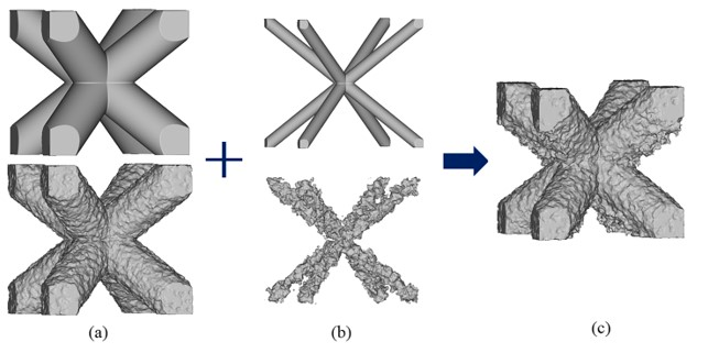
The study outlined below shows how XCT can be applied to extract surface roughness from an AM lattice.
Example of a Boolean subtracted one-unit cell of an AM lattice (a) obtained using XCT showing different up (b) and down skin (c) surface roughness.
Accounting for expected surface roughness
In a study conducted by Younes Chahid, the team performed a complete factorial Design of Experiment (DOE) to correlate nTop surface roughness block parameters (frequency, amplitude, seed) with the conventional engineering ISO 25178 areal surface parameters (Sa, Sq, Sp, Sv, Spd). The study generated a total of 54 DOE surfaces on both planar and cylindrical geometries.
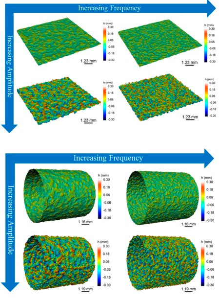
Example of surface roughness design with increasing amplitude, frequency, and fixed seed on both planar and cylindrical surfaces.
The results of the study show a successful correlation between the frequency parameter and the conventional areal surface parameter “Spd”, and a separate correlation between amplitude and a developed “max(Sp, Sv)” parameter (also to Sa and Sq). These results demonstrate that it is possible to design surface roughness on CAD models using areal surface roughness parameters in such a way as to replicate the surface produced during Powder Bed Fusion.
To design surface roughness on CAD models of lattice structures, Chahid developed two workflows. One to extract surface roughness from an AM lattice using XCT and another to design a different upper and down skin surface roughness on a strut-based lattice, as seen below.
Workflow of adding up skin and general surface roughness (a) combined (c) with down skin one (b) using areal surface parameters as inputs (Spd, Sa, Sq…) and a custom nTop workflow.
The result was a CADwDS with a closer surface roughness and smaller mean deviation to the XCT of the AM lattice compared to the original perfect CAD versus the XCT. You can find more information in the published research paper, parametrically designed surface topography on CAD models of additive manufactured lattice structures for improved design validation.
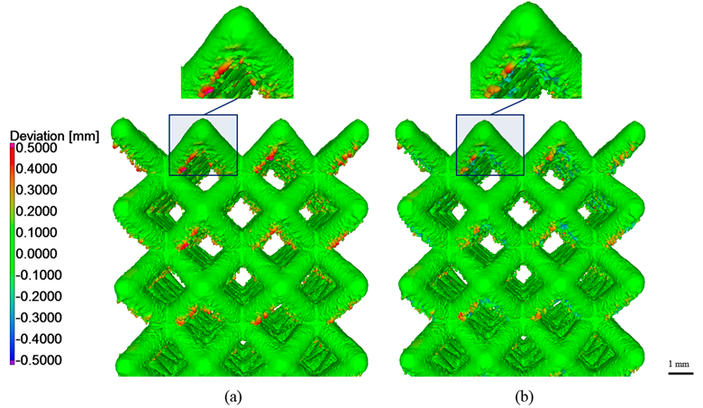
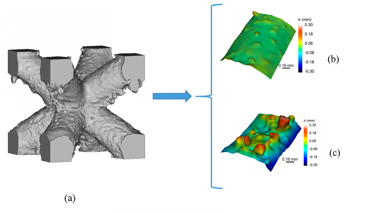
Color map of the deviation analysis of the XCT vs. original CAD (a) and of the XCT vs. CADwDS (b) showing less deviation.
The research in this field will enable the design of virtual CAD models that contain a realistic and better expectation of the anticipated defects or deviations prior to the AM process. This research will assist in the design validation process and enable the cost-effective assessment of different printing parameters, strategies, surface treatments, and behavior of AM parts.
Key takeaways
- The advancement of AM allows us to materialize ideas and designs previously thought impossible to manufacture. But the complexity of AM introduces new challenges that need to be considered when designing and measuring medical implants for AM.
- Often, the complexity of AM designs means they are not measurable using conventional metrology tools, which may require the use of x-ray computed tomography.
- When designing medical devices for AM, it is crucial that you consider both DfAM and metrology rules while creating a design that works specifically for the concerned patient. nTop can help you achieve this.

nTop
nTop (formerly nTopology) was founded in 2015 with the belief that engineers’ ability to innovate shouldn’t be limited by their design software. Built on proprietary technologies that upend the constraints of traditional CAD software while integrating seamlessly into existing processes, nTop allows designers in every industry to create complex geometries, optimize instantaneously, and automate workflows to develop breakthrough 3D-printed parts in record time.
Related content
- VIDEO
Topology Optimization Design for Cast and Injection-Molded Parts
- VIDEO
Lightweighting an impeller for additive manufacturing
- GUIDE
Download: Advanced design software and additive manufacturing for personalized implants
- VIDEO
Sneak peek into the nTop + Autodesk Fusion 360 integration
- ARTICLE
Optimizing thermal management with conformal cooling to extend operational life